The last topic that is important in manufacturing is the issue of partial field. Normally, a mask will not have only one chip. One chip may be of 3 mm x 5 mm size, but a mask can be much larger. Then one mask will have multiple copies of a chip (see figure 2.18). The large box is the mask. The smaller boxes represent the chips. The gaps between the chips, and the border areas are used for keeping alignment marks. During the lithographic process, one exposure of this mask is called “field” or “shot”. The alignment marks are actually placed in the ‘gaps’ between the chips or at the corners of the field.
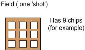
Figure 2.18. Example “field” or “shot”
Two questions arises right away. 1. “Why not make the mask very large and make hundred chips in it?” 2. “On the other hand, why not make a small mask with only one chip?”
We cannot make the mask very large because the size of the lens is not unlimited. For very large lenses, the cost becomes very high. Beyond a limit, we cannot make the lens very large even if money is not a constraint. Thus, the size of the mask is limited by the size of the lens that we can make.
It is possible to make a small mask containing only one chip. However, one has to remember that in the lithographic process, the printing is done step by step. i.e. the mask is brought on top of wafer, aligned to one spot and light is switched on for a controlled time. Then the mask is moved on to the next part, aligned, exposed and so on. So, it is a time consuming process. During production, through put, (i.e. the number of chips produced per hour, or number of wafers processed per week) has to be high. The lithography equipment are very expensive, of the order of Rs. 5 crores (in 2010), and one cannot afford to buy too many of these equipment. Hence, it is necessary to maximize the utilization and minimize the time spent per wafer in these expensive machines. In one exposure or “shot”, if many chips can be made, then the total time will be saved. We also know that we cannot make a very large mask because of limitations on the size of lens. So, one makes the mask of the maximum acceptable size based on lens limitations, and within that, fit as many chips as possible. In this example, it is nine chips.
With this background, we will look into the issue of partial field. The wafer is a circular piece, but a mask is a rectangular piece. It is obvious that in most exposures, all the nine chips square can be fitted into the wafer very nicely, but near the wafer edge, some of the chips will fall outside the wafer. These exposures are called “partial fields”.

Figure 2.19. Partial fields and full fields in a wafer
In the figure 2.19, for convenience, different colors are used to show the full field and partial fields separately.
What is the problem with partial field? First, when we align the mask to the previous layer, we use the alignment marks, which will be on all four corners of the mask (field). In partial field, only one or two corners will fall within the wafer and the rest will be outside the wafer. There is no “previous layer” outside the wafer and hence the alignment has to be done with only one or two marks, which makes it difficult. Second, the focusing is done automatically by the equipment for all exposures. In full field, all the image will fall on the wafer while in partial field, part of the image falls outside the wafer. This makes it difficult for the equipment to focus and this leads to poor image quality.
Just because partial field is problematic, one can not leave these areas empty. It is a useful wafer area. Also, we saw that presence or absence of a line will affect lithography process and that it can be corrected using OPC. Similarly, the presence or absence of patterns will affect neighboring areas. i.e. If partial field areas are left as blank, it will affect the neighboring full field also during the subsequent process. Thus it is better to expose these areas also so that these areas will have at least some images even if they are not perfect images. The alignment and focusing algorithm used by the machine can be modified to control the partial field shots better. One can also optimize the position to some extent, but beyond that not much can be done. There will always be some area which falls in the partial fields. One should be aware of this when they estimate the yields for the production of a particular chip. The details of yield will be discussed in the later chapter.
|