We saw that the lithographic equipment is also called a stepper because it exposes one part of the wafer to the light, and then moves or steps to the next location and repeats the exposure. Recently, a more sophisticated technique called scanning is used. In this, the exposure is not done in one shot. Instead, once the mask is positioned above the wafer, light is shone on only a part of the mask and the wafer. Then the wafer and the mask are moved, as shown in figure. This step is called scanning. When the entire mask is covered, the scanning is completed. Then the wafer is moved to the next step and the scanning continues. Thus, even though the equipment is called as scanner, it is actually a step-and-scan technique.
What is the need for scanning? Large lenses, free from aberrations, are extremely expensive. If only a stepper is used, then for a given mask size, a very large lens is needed. The diameter of the lens must be at least 1.4 times the size of the mask.

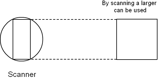
Figure 2.8: A scanner can handle a larger mask than a stepper (when both of them use the same sized lenses).
However, if scanning is available, then the task can be accomplished using a smaller lens. Consider the following example. During scanning, only a part of the mask is exposed. In this example, the entire ‘width’ of the mask is exposed at all the times, but only a small part of the ‘width’ is exposed. By moving the mask (and also the wafer), the entire mask can be covered while using a smaller lens. Even within this small lens, only a small part should be absolutely free from aberrations. Thus for a given mask a smaller lens can be used in step-and-scan systems. Alternatively, for a given lens, a larger mask can be used in a scanner while only a smaller mask can be used in a stepper.
Litho is a critical step in IC manufacturing. Many a times, the failure in the chip occurs because of some problem in litho. In other processes, there may be a way to compensate if any minor deviation occurs. For example, in deposition, if more material is deposited than necessary, then it is possible to adjust for it in the subsequent removal steps. We can remove a bit more than normal and we will be left with a good structure. In litho, if the problem is caught before etching, then we can completely remove all the resists and send
the wafer back for reprocessing. If there is mistake in the litho step, and if the wafer is etched, it is almost impossible to recover. If any dust falls on the wafer during the litho process, the defect will most likely lead to failure. Thus the litho area has to be maintained much more cleaner than all other locations in the fab.
|