The layout file is then placed in a mask writer machine. What is a mask? It is like a stencil, where a flat plate is taken and holes of desired shapes or letters are cut in it. If we place the stencil on top a paper and paint it, the shapes or letters will come nicely and this can be done over any number of papers to get identical results. Instead of cutting holes, the mask has transparent areas which allow light and certain areas which block the light. A schematic of the mask is given in Figure 2.2
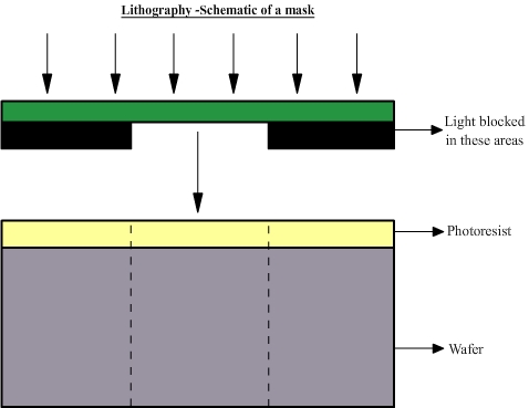
Figure 2.2 Schematic of a mask with wafer and photo resist
Based on the information in the layout file, a mask will be created for each layer. For example, active sites will have a mask and the gate will have a different mask. The mask making is done as follows: A glass plate with chromium deposited on top of it is used as the base. On top of the chromium, a chemical sensitive to electrons is coated. This is called ‘resist’. Then a beam of electrons is directed towards areas (rectangles) that should be open. Electron beam scans the whole mask and whenever the mask is supposed to be ‘open’, the electron beam is ON. Whenever the mask is supposed to block the light, the electron beam will be off. This way, the whole mask is written point by point or ‘pixel by pixel’. Mask making is a tedious work which takes about a day. If there is any small error in the mask, it can be ‘repaired’, but large errors will lead to remaking the whole mask. Masks with very small features are very expensive and the cost of making them is of the order of a million US dollars (about Rs. 5 crores ). The masks are usually not made in the fabs where the ICs are made. Instead mask making is handled by a different department or even outsourced.
|