Once the mask is made, it is used in the photolithography tool. Sometimes the tool is also called as “litho”. It is roughly 12 ft long, 12 ft wide and 8 ft tall. Here, an explanation is of order. If we say ‘car’, it can mean a very small car or a very large car. Similarly all the tools in IC manufacturing come in different sizes. Here we mention the size to give some rough idea. We do not mean that all the lithography tools will be exactly of the size mentioned here.
In litho tool, only one wafer is processed at a time. Its principle is very similar to taking photo using conventional cameras with film. When a camera film is used, first the film has to be inserted into the camera. Next the shutter is opened for a short time, and wherever the light falls on the film, some chemical reaction occurs. In the places where light doesn’t fall, no chemical reaction occurs. (Figure 2.3a)
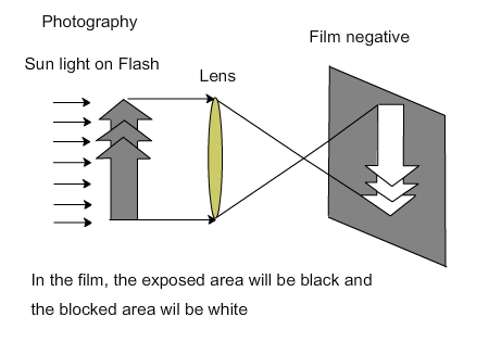
Figure 2.3 a. Creating a photographic negative

Figure 2.3 b. Obtaining prints from a negative
After the photo is taken, the film has to be developed and it has to be done in a dark room. In a black and white film, wherever light has fallen, the film will be dark and wherever light is blocked, the film will be transparent or white. So, it is called a negative. Using a negative, we can make many copies of the photo. For that, a paper with light sensitive coating is needed. When we place the negative on top of the paper and shine light, the areas which are black will block the light and the transparent areas will allow the light (Figure 2.3 b). This light will cause reactions on the chemical coating on the paper. After this, the light sensitive paper is washed or developed in a suitable chemical solution and the photo will be ready.
To create larger or small photos from a negative, the light is passed through a lens. Then we can obtain a larger or smaller photo from the same negative. Likewise, the mask is used as negative in the IC manufacturing. Instead of paper, we use chemical coated silicon wafers. The chemical will be sensitive to light. Typically, the features or shapes on the mask will be four or five times larger than that on the wafer. The features are ‘shrunk’ on the wafer using a lens system. After the wafers are exposed to light in the litho tool with mask, the wafers are usually sent for ‘etching’. This is the summary of photolithography process. We will see the details below.
Why are the masks four or fives times larger than the image on the wafer? It is easier to make larger features on the mask. With this mask, all the layout features will shrink in size on the wafer. Any irregularities in the mask or any dust particle falling on the mask will also be shrunk and hence the image will be affected less. |