In the manufacturing steps, we saw that materials have to be removed only in certain places. The process enabling us to define these places is lithography. The complete name is photolithography, but it is also called as lithography or litho in the industry.
Consider the process flow given in Figure 2.1
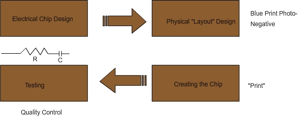
Figure 2.1. Overall flow in chip manufacturing process.
Let us assume that the circuit has been designed and the layout is also generated. The layout will be a file in the computer. This information will be used to generate masks. The masks can be thought of as photonegatives. Using these negatives, any number of photos (i.e. chips) can be generated. We will see the details of the layout file, mask making and chip making here.
Layout:
Just like we call the Microsoft word® file as “doc” file and acrobat® portable document format as “pdf” file, these files have certain standard extensions. GDS is one popular format for the layout file.
The transistor locations are called active sites. An IC will have many layers such as active, gate, metal-1 for the first layer of interconnect metal lines etc. Hence, the gds file of the chip will have information for all the layers. Many parts of the chips can be repetitive. For example, in a memory chip (RAM), the circuit used to store the information is called a bit. The chip will have millions of identical bits where 1’s and 0’s can be stored. All these bits will have identical circuit. It is not necessary to store the layout information of each bit in the gds file. It is sufficient to store the information of one bit and then refer to it or give a pointer to it in other locations. This way of storing information is called ‘hierarchical’.
We will consider an analogy to understand this. For example, in a small company, there may be 20 operators, 5 supervisors, 2 managers and one managing director. Let us assume that all the persons in a certain designation are paid identical salary. Let us also assume that one supervisor and four operators working under the supervisor are called as “group”. If we want to compute the total salary expense in a month for the company, it is sufficient to know the salary of one operator, one supervisor, one manager and one managing director to calculate it. For this purpose, it will be redundant and a waste of effort to describe the details of the salary of every individual separately. In fact, if we know only the ‘group salary’, and the salary of a manager and the managing director, it is sufficient to calculate the total monthly salary expense. We do not even need to know the salary of an individual operator. On the other hand, if an individual operator falls ill and another operator does an extra shift, we need to know the identity of individual operators to calculate the salary for that month correctly. Thus, there are some occasions where individual level information is not necessary and group level information is sufficient; there are also occasions where individual level information is necessary.
Similarly, a small group of transistors can be stored as ‘circuit 1’ and another different group of transistors may be grouped as ‘circuit 2’ and yet another as circuit 3. A combination of circuit 1 and 2 may be grouped as ‘higher level 1’ By this arrangement, the layout file size will be significantly reduced, for most of the designs. Even with this reduction, the typical layout file sizes are a few gigabytes. To describe the overall layout, hierarchical format is preferred. In order to perform complicated tasks such as optical proximity correction (OPC), which will be described in the later section, the full detailed format is necessary. The complete detailed layout is sometimes called as “flat” file, in contrast to the “hierarchical” file. |