Cu metallization – Process integration: Copper has lower electrical resistance and higher electromigration resistance then aluminum. Hence it was introduced as interconnect material in the 1990s. Dry etching of copper was difficult and hence the aluminum process integration scheme could not be used for copper. A new set of processes and sequence was needed. The following describes the process integration scheme of copper metallization.
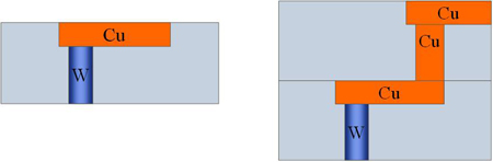
(a) (b)
Fig 9.5. Schematic of chip in BEOL , with Cu line (a) after M1 layer (b) after fabrication of via12 and M2 layer
At first, a thin layer of silicon nitride is deposited on top of copper, by LPCVD as shown in Fig 9.6 a. Next, a thick layer of silicon dioxide is deposited on top (Fig. 9.6 b). Both the silicon nitride and silicon dioxide are insulators. In the next step, using lithography and dry etching, holes for the vias are created (Fig 9.6 c). In this process, the etching ‘stops on nitride’. i.e. only the oxide layer is removed but the nitride layer is not removed. The etching chemicals and process conditions are chosen such that only the oxide will etch.
Then, again using lithography and dry etching, trenches for metal lines are made (Fig. 9.6 d). This is called as ‘blind etch’ because the etch does not stop at another material. The etching time is controlled so that the expected depth (with some variation) will be created.
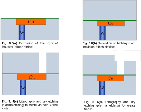
After this step, thin layer of the silicon nitride, inside the via hole, is removed using dry etching using suitable combination of chemicals and plasma (Fig. 9.6 e). During this etch, a slight damage to Cu lying below may occur. However, since the nitride layer is thin, the etch time will be very short and the damage is also limited. If the nitride layer were not present and only oxide were used as insulator, the potential damage to Cu line would be severe.
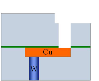
Fig. 9. 6(e), Dry etching (plasma etching) to remove nitride at the bottom layer
Subsequently, a thin layer of barrier (Ta/TaN, and in some cases, an additional layer of Ru) is deposited (Fig. 9.6 f). This is needed to prevent the diffusion of Cu through the silicon dioxide insulator. Then, another thin layer of Cu is deposited using CVD method (Fig. 9.6 g). This is needed to obtain a layer of at least moderate electrical conductivity for the next step.
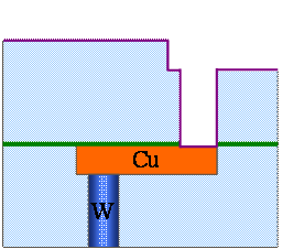
Fig. 9.6(f), Ta/TaN deposition by PVD
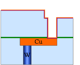
Fig. 9. 6(g) Cu seed layer deposition by CVD (or PVD)
After the seed layer is deposited, a thick Cu layer is deposited using electrochemical deposition (Fig 9.6 h). The Cu formed has larger crystals, lower electrical resistance and higher electromigration resistance compared to Cu deposited by other methods such as PVD or CVD. The Cu can not be deposited only inside the vias and trenches. Hence it is deposited throughout the wafer surface. Then in the next step, the excess Cu is removed using CMP (Fig. 9. 6 i)
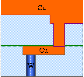
Fig. 9. 6(h) Cu deposition by electrochemical deposition
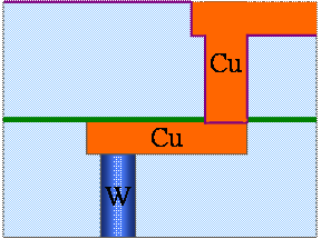
Fig. 9. 6(i) Removal of excess Cu by first stage of CMP- (Main Cu CMP)
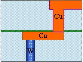
Fig. 9. 6(j) Ta/TaN (barrier layer) removal by 2nd stage of CMP (Barrier CMP)
The removal is done in two steps. In the first step, only the Cu is removed. The barrier and the insulator are not removed (Fig. 9.6 i). In the second step or 2nd stage of the CMP, a different slurry is used and the barrier metal is also removed in the unwanted places (Fig. 9.6 j). Subsequently, the Cu is annealed so that the crystal size increases.
This scheme of intergration is called “via first” integration because via holes are made before trenches here. In another process sequence, the trenches can be made first and the vias can be made afterwards (i.e. the processes in Fig. 9.6 c and Fig. 9.6 d can be done in reverse order) and that scheme is called “trench first” integration. Most fabs use the via first scheme for copper metallization.
Summary: Process integration denotes combining various processes to obtain the desired structure, to obtain a functioning chip, in a robust fashion. In the modern chips, the BEOL part plays a significant role in determining the yield as well as the speed of the chip. Electromigration is the movement of metal atoms due to the movement of electrons. It can cause failures at the later stage of chip operation and hence is a reliability issue. If the metal lines are long, and/ or if large current densities are used, then the chances of failure by electromigration is high. It is desirable to have high electromigration resistance and low electrical resistance. Aluminum has more electrical resistance than Cu and less electromigration resistance than Cu. However, it can be etching using plasma and a process sequence using tungsten vias and aluminum metal lines was used to make interconnects. With the introduction of CMP, it is possible to make Cu vias and Cu metal lines on chips, and the different process sequence needed to obtain Cu interconnects was discussed. |