Aluminum process: When aluminum is used as interconnect material, a layer of titanium and titanium nitride is used as a barrier and adhesion promoter. This prevents the diffusion of aluminum atoms through the insulator. The insulator material used is SiO2. The sequence of process steps needed to fabricate a via and a metal line are given below.
Let us assume that the fabrication of M1 is completed and that via12 and M2 have to be fabricated. i.e. the chip is at the stage as shown in Fig.9. 2(a) and we need to process it so that it becomes as shown in Fig 9. 2(b).
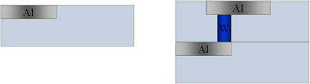
Fig 9.2. Schematic of chip in BEOL (a) after M1 layer (b) after fabrication of via12 and M2 layer
First, a layer of silicon dioxide is deposited on top of M1 (Fig 9.3a). Then using lithography and plasma etching, via12 hole is made (Fig 9.3b). Next, a thin layer of TiN/Ti is deposited on top. This film is formed on the top of the surface as well as on the sides and bottom of the via hole (Fig 9.3c). Then, W is deposited using CVD (Fig 9.3d). Excess W is removed using CMP (Fig 9.3e).
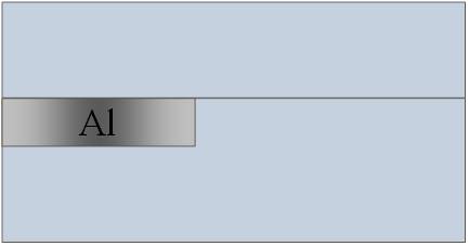
Fig. 9.3(a) Deposition of insulator (silicon dioxide)
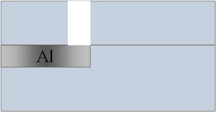
Fig. 9. 3(b) Lithography and dry etching (plasma etching) to create via hole
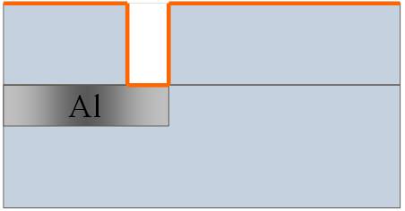
Fig. 9. 3(c), Ti/TiN liner deposition by PVD
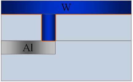
Fig. 9.3(d), Tungsten deposition by CVD
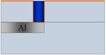
Fig. 9. 3(e) Removal of excess tungsten by CMP
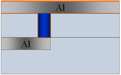
Fig. 9. 3(f) Deposition of aluminum and Ti/TiN liner by PVD
In the next step, aluminum and titanium are deposited on the top. After that, using lithography and plasma etching, aluminum is removed from unwanted locations. The titanium barrier layer is also removed along with aluminum in those locations.
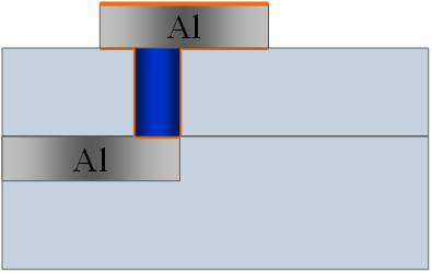
Fig. 9. 3(g) Lithography and dry etching to remove excess aluminum and Ti/TiN liner
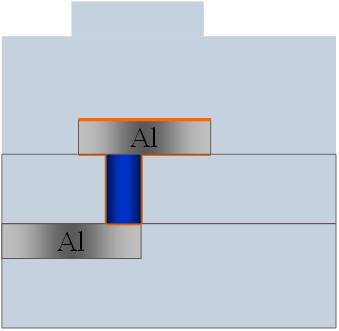
Fig. 9. 3(h) Deposition of insulator (silicon dioxide) by CVD
Oxide layer is deposited on top of the aluminum and the non-planar surface is subjected to CMP, to make it planar. This is necessary so that subsequently lithography can be done on the surface with minimal distortions.
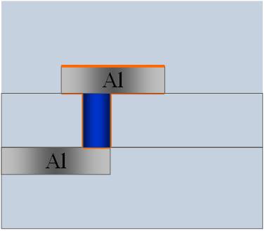
Fig. 9. 3(i) Planarization of the insulator layer by CMP
ESD and Antenna effect: Electrostatic discharge (ESD) is a phenomenon of importance in aluminum plasma
etching. When charge builds up in a material, it is called static charge. It is usually found in insulators. As an example, if a glass rod is rubbed against a woolen cloth, it will build up static charge. It also varies with the environment: in humid atmospheres, the charge build up is low, whereas in dry environments, the charge build up is high. After rubbing the glass rod against wool, if the glass rod is brought near a metal, then the excess charge be discharged and a spark may be seen.
During aluminum etching, plasma is used and the presence of electrons and ions in the plasma causes the aluminum surface to be charged. Since aluminum is a conductor, the charge density is usually not high when the entire surface is exposed to plasma. However, sometime during etching, aluminum lines begin to be separated and finally when the etching is completed, many short metal lines and a few long metal lines would be formed.
We notice that the aluminum lines are connected to transistors and diodes. If too much charge builds up in the aluminum, then the diode or transistor may breakdown. This unwanted phenomenon is called ESD in IC manufacturing. If the metal lines are long, then they act as an antenna and collect more charge. This is called antenna effect. To minimize the problems due to this, during the design stage itself, the maximum length of the metal line will be limited. Similarly, in the design stage, a few diodes with certain specific characteristics will be added to the circuits so that if ESD occurs, then only those diodes will break down. These are sacrificial diodes and are sometimes called as ESD protection diodes. They are not part of the actual functioning of the chip and are present only to protect other transistors and diodes during the metal etching by plasma.
|