Sheet resistance: When the wafer is doped, the conductivity of the material increases. The level of doping can be estimated by measuring the conductivity. In IC industry, a quantity called sheet resistance is often measured and reported. Here we will learn about the concept of sheet resistance.
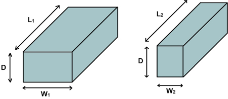
Figure 6.9. Schematic of two lines with the same depth, but different lengths and widths.
Consider two metal lines of same depth (D), but with different width and lengths. For example, in metal 2 layer, the depth is given by the deposition process, but the length and widths of lines are given by the lithography process (mask). Hence all lines in metal 2 will have same depth but different length and widths.
A top view of the same lines will appear as follows.
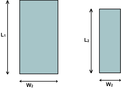
Figure 6.10. Top view of the two lines shown in fig. 6.9
The resistance of the first and second lines are given respectively by
 and and  , where r is the resistivity of the material. Since the depth is the same for both lines, the resistance is proportional to the ratio of length to width. The ratio of resistivity to depth is called “sheet resistance”. The ratio of length to width is also called “number of squares”. When the ratio of length to width is one, then the top view will appear as a square. For a given layer, the resistance of each square is the same, regardless of the size of the square. , where r is the resistivity of the material. Since the depth is the same for both lines, the resistance is proportional to the ratio of length to width. The ratio of resistivity to depth is called “sheet resistance”. The ratio of length to width is also called “number of squares”. When the ratio of length to width is one, then the top view will appear as a square. For a given layer, the resistance of each square is the same, regardless of the size of the square.
In the top view, if we try to fit a large square in the rectangle, the first line can accommodate two large squares. The second line can accommodate three squares
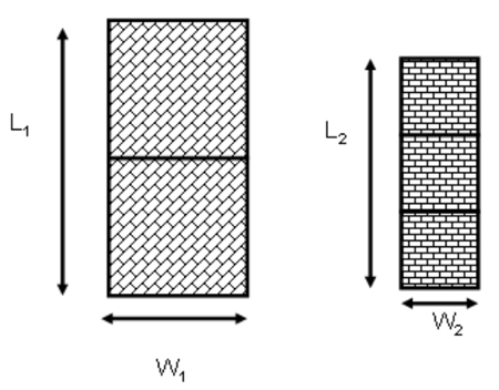
Figure 6.10. Top view of the two lines shown in fig. 6.9, with number of squares illustrated
For a given layer (i.e. when the material and the depth are fixed), the sheet resistance is a constant and is expressed as ‘ohm/square’ or sometimes written as “ohm/□’. Then the resistance of a line is calculated as the product of sheet resistance and the ‘number of squares’ in the line (from the top view).
|