Physical Vapor Deposition:
DC sputtering
The PVD equipment will be about 4 ft in height and 4 ft in diameter. The material to be deposited (e.g. titanium) will be at the top, as shown in schematic Fig 3.1
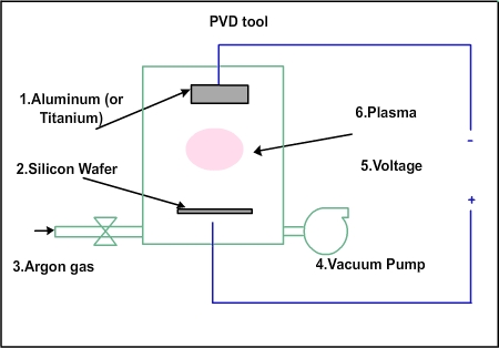
Figure 3.1. Schematic of a PVD chamber
The tungsten will be in the form of a disc of 1 inch thickness and 5 or 6 inches diameter. At the bottom, silicon wafer will be kept. Apart from these, there will be facilities to allow gases into the chamber and to evacuate the chamber with vacuum pump and electrical connections to apply very high voltage (of the order of 10000 V). The negative plate will be near the tungsten and the positive plate will be near the wafer. Tungsten (or any other material in its place) is called target. Why is it called target? How is it deposited onto the wafer?
Let us consider an example. In old houses, if we stand inside the house and throw a ball at the top of the house, some of the dust material will fall on the floor. If we throw the ball repeatedly, after some time, the whole floor will be covered with dust. Some dust particles may be coarse and may not stick well to the floor. The fine dust particles will stick well to the floor.
In PVD, we can visualize a similar process: Instead of the ball, argon ions are used. The ceiling represents the tungsten target. When the ions hit the target, a few atoms will break away from the target and fall on the wafer. This is a very simplified description of PVD process. PVD is also called sputtering.
First the air in the chamber must be removed and vacuum must be created. Then argon gas sent inside and a low pressure will be maintained. If high voltage is applied to the plates, a plasma will be generated. The plasma will have electrons and positive argon ions. The plasma cannot be generated by normal 230 volts. The positive argon ions will be attracted towards the negative plate. They will move towards the negative plates and hit the tungsten with high force. That is why tungsten is called target in this process.
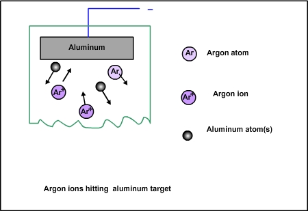
Figure 3.2. Argon ions hitting the target
Since the argon ions impinge on the target with large force, some of the target atoms will break and come out , as shown in Fig 3.2. How many tungsten atoms will come for each argon ion hitting the target? This number is called sputtering yield. It depends on the speed of the argon ions, the angle of the impact and also on the bond strength of the target. Tungsten is one of the hard materials. If a relatively soft material such as copper is used as target, then the yield will be higher.
The atoms from the target will come towards the wafer with some force. Not all of them will deposit on the wafer. Some will be deposited (Figure 3. 3), while some will bounce back (Figure 3.4). Some may even bounce back and remove some of the materials already deposited on the wafer (Figure 3.5)
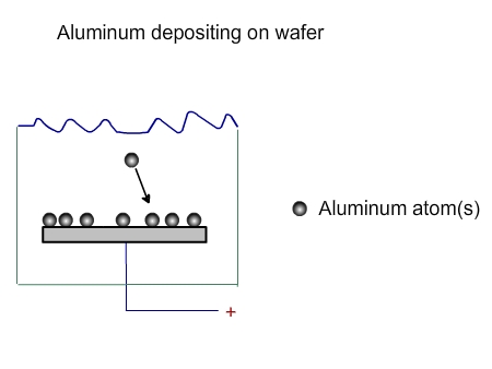
Figure 3.3. Processes near wafer in a PVD chamber. Deposition
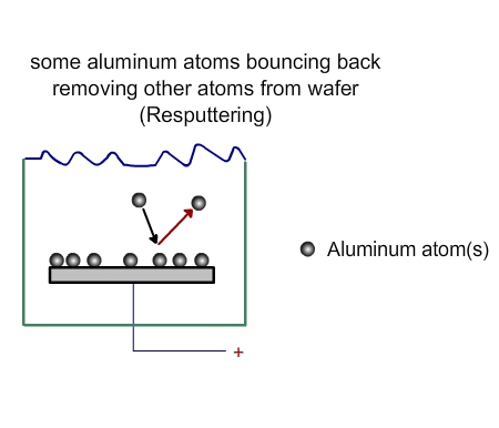
Figure 3.4 Processes near wafer in a PVD chamber. Bounce back
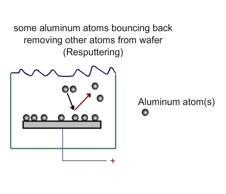
Figure 3.5 Processes near wafer in a PVD chamber. Resputtering
Among the tungsten atoms that fall on the wafer, the fraction that stick to the wafer is called sticking coefficient. If all the atoms that fall on the wafer stick to it, then the sticking coefficient is one. If none of them stick, then the sticking coefficient is zero. Typically, the sticking coefficient is about 0.7 to 0.8.
|