Under etch and over etch:
Let us consider an example to understand the dry etching used in IC manufacturing. Consider the schematic in fig 4.4. Here the copper wire at the bottom must be connected to the higher level. For that, the glass has to be etched at the right place. Then copper must be filled in the hole. We will consider only the etching part here. In the Figure 4.4, a hole needs to be etched or drilled through silicon dioxide, from the top in only one direction. It has to stop exactly at the copper level. If it etches less, it is ‘under etch’ and if it etches more, it is over etch. Both are problematic. If it etches in all directions, that is also a problem.
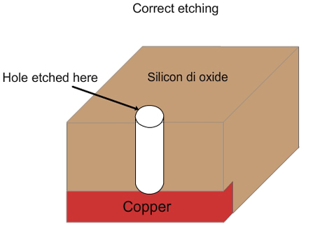
Figure 4.4. Example of correct etch.
In case of under etch, there will be some silicon dioxide left (Figure 4.5). Even if copper is deposited in the hole, it will not connect to the bottom copper line. So, the circuit won’t be complete and the IC will not work.
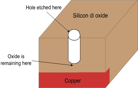
Figure 4.5. Schematic of under etch
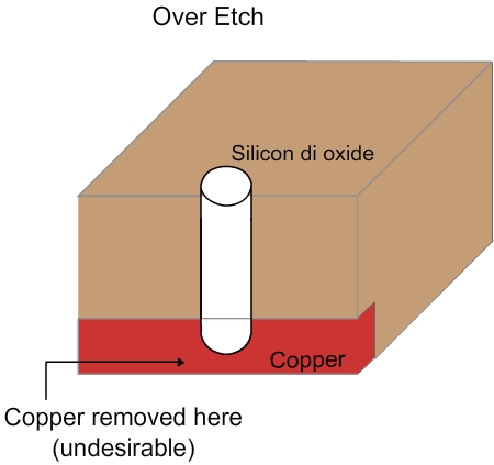
Figure 4.6. Schematic of over etch
In over etch, the copper line at the bottom will get corroded and may even completely disappear (Figure 4.6). This will also lead to the failure of the chip. Also, if the etching happens in all directions, there may be a problem that it will touch a neighboring contact. So, unidirectional etching is essential.
Normally, a few wafers will be etched for various times (e.g. 60 seconds, 90 seconds, 120 seconds etc) and the average removal rate would have been calculated based on those. From these values, the etching tool can be operated for a specific time so that the material can be removed up to the desired depth. Even then, there might be some variation in the etching and hence usually the tool is operated for at least 10% longer than the estimate. This is called “over etch”.
If the etching is continued for 10% more time, then won’t it remove the copper at the bottom? Yes, it will. In order to prevent it, there would be a silicon nitride layer on top of copper and below the silicon dioxide, as shown in figure 4.7. The silicon nitride layer will not be easily removed by the chemicals used in silicon dioxide etching. Hence 10% over etch of silicon dioxide will not remove the silicon nitride. After silicon dioxide is etched, the silicon nitride will be etched using dry etching, with different chemicals. Since the silicon nitride layer thickness is very small, the etching time is also very small and it can be etched with good control. Hence the problems due to under etch or over etch will not be there.
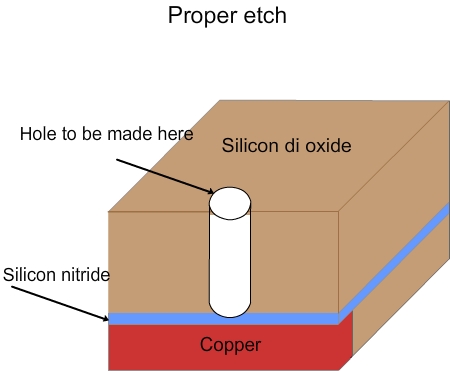
Figure 4.7. Schematic of proper etch using nitride layer in the process flow
|