Devices offering high resistance at low voltages and low resistance at high voltages.
-
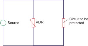
Used to protect a circuit against sudden upsurges in the voltage or transients (Figure 3.7)
Typically used materials are ZnO and SiC powders bonded in a matrix with an intergranular layer that is highly resistive. The current-voltage characteristics are governed by the electrical nature of grain and intergranular layers.
-
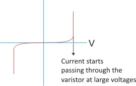
The basic principle of operation is that the material's resistance is high at low voltages and decreases when voltage is increased, allowing excess currents to pass through thereby protecting the circuit (Figure 3.8).
| Figure 3. 7 Schematic diagram showing use of varistor in circuit protection |
| Figure 3. 8 Current (I) - Voltage (V) characteristics of a varistor |
-
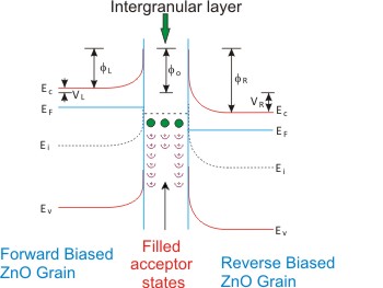
For example, zinc oxide particles of size about 10-50 µm are mixed with other oxides such as bismuth or manganese oxides which form a highly resistive intergranular layer of thickness between 1 nm to 1 µm between zinc oxide grains.These IGLs contain defect states whose role is to trap free electrons from the neighbouring n-type semiconducting zinc oxide grains. This results in the formation of a space charge depletion layer in the ZnO grains in the region adjacent to the grain boundaries as shown in the figure. These boundaries between each grain and its neighbor forms a junction showing diode like characteristics and allowing flow of current in one direction only (Figure 3.9).
In the figure, the left-hand grain is forward biased by a voltage VL, and the right side is reverse biased to VR. The respective barrier heights are φL and φR while the zero biased barrier height is φ0. As the voltage bias is increased, φL is decreased and φR is increased, leading to a lowering of the barrier and an increase in conduction.
The whole mass of material resembles an electrical circuit network with back to back pair of diodes, with each pair of diode in parallel with many others. Very small current flows when a small voltage is applied across the electrodes which is mainly caused by reverse leakage through the diode junctions. When voltages are high enough to cause break down of the diode junction, large currents flow due to thermionic emission as well as tunneling, as seen in the above graph.
| Figure 3. 9 Schematic of the electronic structure of ZnO grain and intergranular layer (note the bias on the grains) |